![]()
|
|
||||||||||||||||||||||||||||||||||||||||||||||||||||||||||||||||||||||||||||||||||||||||||||||||||||||||||||||||||||||||||||||||||||||||||||||||||||||||||||||||||||||||||||||||||||||||||||||||||||||||||||||||||||||||||||||||||||||||||||||||||||||||||||||||||||||||||||||||||||||||||||||||||||||||||||||||||||||||||||||||||||||||||||||||||||||||||||||||||||||||||||||||||||||||||||||||||||||||||||||||||||||||||||||||||||||||||||||||||||||||||||||||||||||||||||||||||||||||||||||||||||||||||||||||||||||||||||||||||||||||||||||||||||||||||||||||||||||||||||||||||||||||||||||||||||||||||||||||||||||||||||||||||||||||||||||||||||||||||||||||||||||||||||||||||||||||||||||||||||||||||||||||||||||||||||||||||||||||||||||||||||||||||||||||||||||||||||||||||||||||||||||||||||||||||||||||||||||||||||||||||||||||||||||||||||||||||||||||||||||||||||||||||||||||||||||||||||||||||||||||||
|
The PICER-LCD-XY1 is an educational electronics kit that allows you to control LCD directly from PIC (PIC16F690) Micro-controller.
The PICER-LCD-XY1, is the fun and easy way to write to Liquid Crystal Display (LCD).
One can program the PIC16F690 Micro-controller Flash memory using his/her PICKIT 2 (sold directly from Microchip Corporation) directly from a personal computer (PC) via our adaptor board the PK2-A3 (sold separately).
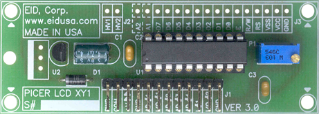
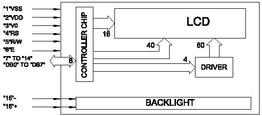
The board utilizes the PIC16F690 IC (20 pin DIP configuration). The board also includes connector (J1) that allows you to connect 4 10-bit ADC lines and a few I/Os. The J2 connector is for those who desire to connect back light LCD.
Do It Yourself (DIY) build a software driven micro-processor base LCD kit, and have a blast!
|
||||||||||||||||||||||||||||||||||||||||||||||||||||||||||||||||||||||||||||||||||||||||||||||||||||||||||||||||||||||||||||||||||||||||||||||||||||||||||||||||||||||||||||||||||||||||||||||||||||||||||||||||||||||||||||||||||||||||||||||||||||||||||||||||||||||||||||||||||||||||||||||||||||||||||||||||||||||||||||||||||||||||||||||||||||||||||||||||||||||||||||||||||||||||||||||||||||||||||||||||||||||||||||||||||||||||||||||||||||||||||||||||||||||||||||||||||||||||||||||||||||||||||||||||||||||||||||||||||||||||||||||||||||||||||||||||||||||||||||||||||||||||||||||||||||||||||||||||||||||||||||||||||||||||||||||||||||||||||||||||||||||||||||||||||||||||||||||||||||||||||||||||||||||||||||||||||||||||||||||||||||||||||||||||||||||||||||||||||||||||||||||||||||||||||||||||||||||||||||||||||||||||||||||||||||||||||||||||||||||||||||||||||||||||||||||||||||||||||||||||||
|
The Kit shown above without the LCD (sold separately)
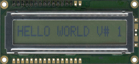
The Kit shown above (front view) connected to 1 line 16 Characters LCD (sold separately)
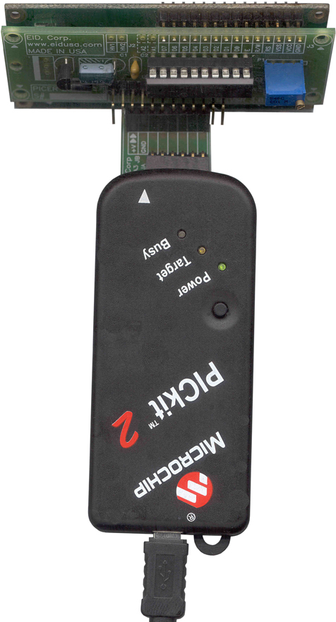
The Kit shown above (side view) connected to 1 line 16 Characters LCD, and PICKITTM 2**.
PICKIT-2, USB cable, connectors and LCD are sold separately
** PICKIT 2 is register Tradmark of Microchip Corp. |
||||||||||||||||||||||||||||||||||||||||||||||||||||||||||||||||||||||||||||||||||||||||||||||||||||||||||||||||||||||||||||||||||||||||||||||||||||||||||||||||||||||||||||||||||||||||||||||||||||||||||||||||||||||||||||||||||||||||||||||||||||||||||||||||||||||||||||||||||||||||||||||||||||||||||||||||||||||||||||||||||||||||||||||||||||||||||||||||||||||||||||||||||||||||||||||||||||||||||||||||||||||||||||||||||||||||||||||||||||||||||||||||||||||||||||||||||||||||||||||||||||||||||||||||||||||||||||||||||||||||||||||||||||||||||||||||||||||||||||||||||||||||||||||||||||||||||||||||||||||||||||||||||||||||||||||||||||||||||||||||||||||||||||||||||||||||||||||||||||||||||||||||||||||||||||||||||||||||||||||||||||||||||||||||||||||||||||||||||||||||||||||||||||||||||||||||||||||||||||||||||||||||||||||||||||||||||||||||||||||||||||||||||||||||||||||||||||||||||||||||||
|
Kit Includes:
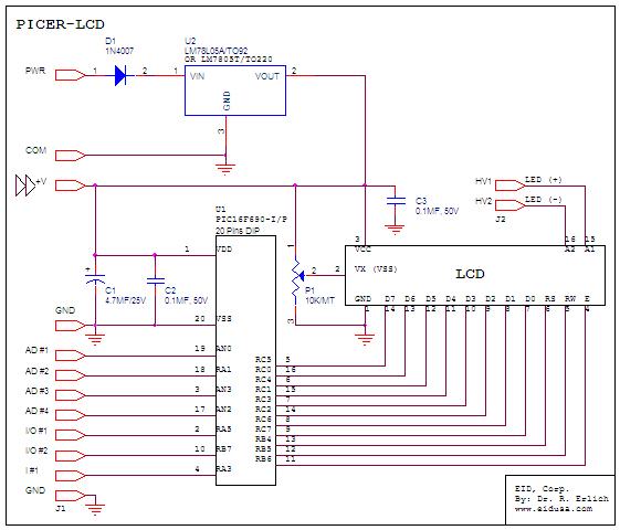
Schematic:
Down load your code directly using your PICKIT2 via our PK2-AD3 adepter sold separately
|
||||||||||||||||||||||||||||||||||||||||||||||||||||||||||||||||||||||||||||||||||||||||||||||||||||||||||||||||||||||||||||||||||||||||||||||||||||||||||||||||||||||||||||||||||||||||||||||||||||||||||||||||||||||||||||||||||||||||||||||||||||||||||||||||||||||||||||||||||||||||||||||||||||||||||||||||||||||||||||||||||||||||||||||||||||||||||||||||||||||||||||||||||||||||||||||||||||||||||||||||||||||||||||||||||||||||||||||||||||||||||||||||||||||||||||||||||||||||||||||||||||||||||||||||||||||||||||||||||||||||||||||||||||||||||||||||||||||||||||||||||||||||||||||||||||||||||||||||||||||||||||||||||||||||||||||||||||||||||||||||||||||||||||||||||||||||||||||||||||||||||||||||||||||||||||||||||||||||||||||||||||||||||||||||||||||||||||||||||||||||||||||||||||||||||||||||||||||||||||||||||||||||||||||||||||||||||||||||||||||||||||||||||||||||||||||||||||||||||||||||||
|
Character Type Liquid Crystal Display (LCD) Modules Features 1.
5x8 dot matrix 2.
Built-in controller (KS0066 or equivalent) 3.
+5V or +3.3V power supply 4.
1/16 duty cycle 5. 8-bit parallel interface
LCD Kit Interface pin Connections information
LCD 16 pins (14 I/O + 2 for Back-light)
Back-light
J4 & J5 I/O or Power indication or LED control:
*** For power indication G short to X
LCD Character Address Code
Code Instruction Set for Character Type LCD Modules
* The module automatically performed initialization when powered on (using internal reset circuit). The following instructions are executed during initialization:
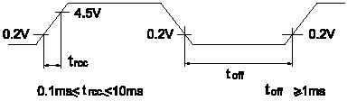
Power On Timing Diagram
Note: When the above power supply condition is not satisfied, the internal reset circuitry does not operate correctly. In this case perform the needed initialization by sending function set instructions thrice from MPU after turning the power on. For example, to designate an 8-bit data length, set the following instructions thrice.
Character Type LCD Modules Initialization For 8 bit data interfacing
Power On
Wait for 15ms or more after Vcc rises to 4.5v Please be advised that BF cannot be checked at this time
Wait for 4.1ms or more Please be advised that BF cannot be checked at this time
Wait for 100us or more
BF cannot be checked at this time, check for not busy
check for not busy
check for not busy
check for not busy
End of Initialization
Character Type LCD Modules Initialization For 4 bit data interfacing Power On Wait
for 15ms or more after Vcc rises to 4.5v. Please be
advised that BF cannot be checked at this time
Wait for 4.1ms or more. Please be advised that BF cannot be
Wait for 100us or more Please be advised that BF cannot be
check for not busy
check for not busy
check for not busy
check for not busy
check for not busy
Check for not busy
End of Initialization
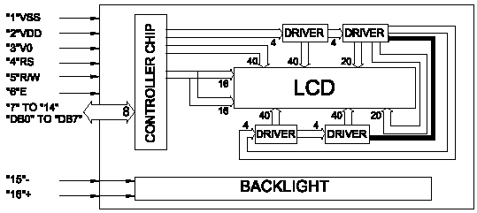
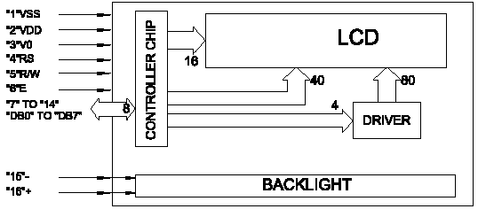
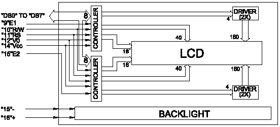
Typical Character Type LCD Modules Block Diagrams 16x1 DMM, 1/16 MUX
Software Tips:
1. W holds the character to move to Port C (The display data lines) DB0 to DB7 (8 Bits)
An example move 'A' --> W --> PORT C
MOVLW 81H ;'A' --> W MOVWF PORTC ;W --> PORT C
See below table for all the ASCII characters:
CA MOVLW 81H ;A SA MOVLW 91H ;a CB MOVLW 41H ;B SB MOVLW 51H ;b CC MOVLW 0C1H ;C SC MOVLW 0D1H ;c CD MOVLW 05H ;D SD MOVLW 15H ;d CE MOVLW 85H ;E SE MOVLW 95H ;e CF MOVLW 45H ;F SF MOVLW 55H ;f CG MOVLW 0C5H ;G SG MOVLW 0D5H ;g CH MOVLW 09H ;H SH MOVLW 19H ;h CI MOVLW 89H ;I SI MOVLW 79H ;i CJ MOVLW 49H ;J SJ MOVLW 59H ;j CK MOVLW 0C9H ;K SK MOVLW 0D9H ;k CL MOVLW 0DH ;L SL MOVLW 1DH ;l CM MOVLW 8DH ;M SM MOVLW 9DH ;m CN MOVLW 4DH ;N SN MOVLW 5DH ;n CO MOVLW 0CDH ;O SO MOVLW 0DDH ;o CP MOVLW 03H ;P SP MOVLW 13H ;p CQ MOVLW 83H ;Q SQ MOVLW 93H ;q CR MOVLW 43H ;R SR MOVLW 53H ;r CS MOVLW 0C3H ;S SS MOVLW 0D3H ;s CT MOVLW 07H ;T ST MOVLW 17H ;t CU MOVLW 87H ;U SU MOVLW 97H ;u CV MOVLW 47H ;V SV MOVLW 57H ;v CW MOVLW 0C7H ;W SW MOVLW 0D7H ;w CX MOVLW 0BH ;X SX MOVLW 1BH ;x CY MOVLW 8BH ;Y SY MOVLW 9BH ;y CZ MOVLW 4BH ;Z SZ MOVLW 5BH ;s N0 MOVLW 12H ;0 N1 MOVLW 92H ;1 N2 MOVLW 52H ;2 N3 MOVLW 0D2H ;3 N4 MOVLW 16H ;4 N5 MOVLW 96H ;5 N6 MOVLW 56H ;6 N7 MOVLW 0D6H ;7 N8 MOVLW 1AH ;8 N9 MOVLW 9AH ;9 DOT MOVLW 5CH ;. COMA MOVLW 1CH ;, DEG MOVLW 0EFH ;Degree EQL MOVLW 9EH ;= AT MOVLW 01H ;@ NUM MOVLW 0D0H ;# SPC MOVLW 30H ;Space
Note: LCD sold separately! |
||||||||||||||||||||||||||||||||||||||||||||||||||||||||||||||||||||||||||||||||||||||||||||||||||||||||||||||||||||||||||||||||||||||||||||||||||||||||||||||||||||||||||||||||||||||||||||||||||||||||||||||||||||||||||||||||||||||||||||||||||||||||||||||||||||||||||||||||||||||||||||||||||||||||||||||||||||||||||||||||||||||||||||||||||||||||||||||||||||||||||||||||||||||||||||||||||||||||||||||||||||||||||||||||||||||||||||||||||||||||||||||||||||||||||||||||||||||||||||||||||||||||||||||||||||||||||||||||||||||||||||||||||||||||||||||||||||||||||||||||||||||||||||||||||||||||||||||||||||||||||||||||||||||||||||||||||||||||||||||||||||||||||||||||||||||||||||||||||||||||||||||||||||||||||||||||||||||||||||||||||||||||||||||||||||||||||||||||||||||||||||||||||||||||||||||||||||||||||||||||||||||||||||||||||||||||||||||||||||||||||||||||||||||||||||||||||||||||||||||||||
|
Description and SKU# |
Price |
Picture |
||||||||||||||||||||||||||||||||||||||||||||||||||||||||||||||||||||||||||||||||||||||||||||||||||||||||||||||||||||||||||||||||||||||||||||||||||||||||||||||||||||||||||||||||||||||||||||||||||||||||||||||||||||||||||||||||||||||||||||||||||||||||||||||||||||||||||||||||||||||||||||||||||||||||||||||||||||||||||||||||||||||||||||||||||||||||||||||||||||||||||||||||||||||||||||||||||||||||||||||||||||||||||||||||||||||||||||||||||||||||||||||||||||||||||||||||||||||||||||||||||||||||||||||||||||||||||||||||||||||||||||||||||||||||||||||||||||||||||||||||||||||||||||||||||||||||||||||||||||||||||||||||||||||||||||||||||||||||||||||||||||||||||||||||||||||||||||||||||||||||||||||||||||||||||||||||||||||||||||||||||||||||||||||||||||||||||||||||||||||||||||||||||||||||||||||||||||||||||||||||||||||||||||||||||||||||||||||||||||||||||||||||||||||||||||||||||||||||||||||||
|
PIC to CHARACTER LCD kit EID-K-PIC-LCD-XY1-ASM Fully assembled |
49.00 |
|
||||||||||||||||||||||||||||||||||||||||||||||||||||||||||||||||||||||||||||||||||||||||||||||||||||||||||||||||||||||||||||||||||||||||||||||||||||||||||||||||||||||||||||||||||||||||||||||||||||||||||||||||||||||||||||||||||||||||||||||||||||||||||||||||||||||||||||||||||||||||||||||||||||||||||||||||||||||||||||||||||||||||||||||||||||||||||||||||||||||||||||||||||||||||||||||||||||||||||||||||||||||||||||||||||||||||||||||||||||||||||||||||||||||||||||||||||||||||||||||||||||||||||||||||||||||||||||||||||||||||||||||||||||||||||||||||||||||||||||||||||||||||||||||||||||||||||||||||||||||||||||||||||||||||||||||||||||||||||||||||||||||||||||||||||||||||||||||||||||||||||||||||||||||||||||||||||||||||||||||||||||||||||||||||||||||||||||||||||||||||||||||||||||||||||||||||||||||||||||||||||||||||||||||||||||||||||||||||||||||||||||||||||||||||||||||||||||||||||||||||
|
EID-K-PIC-LCD-XY1-KIT Kit only |
39.75 |
|
||||||||||||||||||||||||||||||||||||||||||||||||||||||||||||||||||||||||||||||||||||||||||||||||||||||||||||||||||||||||||||||||||||||||||||||||||||||||||||||||||||||||||||||||||||||||||||||||||||||||||||||||||||||||||||||||||||||||||||||||||||||||||||||||||||||||||||||||||||||||||||||||||||||||||||||||||||||||||||||||||||||||||||||||||||||||||||||||||||||||||||||||||||||||||||||||||||||||||||||||||||||||||||||||||||||||||||||||||||||||||||||||||||||||||||||||||||||||||||||||||||||||||||||||||||||||||||||||||||||||||||||||||||||||||||||||||||||||||||||||||||||||||||||||||||||||||||||||||||||||||||||||||||||||||||||||||||||||||||||||||||||||||||||||||||||||||||||||||||||||||||||||||||||||||||||||||||||||||||||||||||||||||||||||||||||||||||||||||||||||||||||||||||||||||||||||||||||||||||||||||||||||||||||||||||||||||||||||||||||||||||||||||||||||||||||||||||||||||||||||
|
EID-K-PIC-LCD-XY1-PCB PCB only |
12.75 |
|
||||||||||||||||||||||||||||||||||||||||||||||||||||||||||||||||||||||||||||||||||||||||||||||||||||||||||||||||||||||||||||||||||||||||||||||||||||||||||||||||||||||||||||||||||||||||||||||||||||||||||||||||||||||||||||||||||||||||||||||||||||||||||||||||||||||||||||||||||||||||||||||||||||||||||||||||||||||||||||||||||||||||||||||||||||||||||||||||||||||||||||||||||||||||||||||||||||||||||||||||||||||||||||||||||||||||||||||||||||||||||||||||||||||||||||||||||||||||||||||||||||||||||||||||||||||||||||||||||||||||||||||||||||||||||||||||||||||||||||||||||||||||||||||||||||||||||||||||||||||||||||||||||||||||||||||||||||||||||||||||||||||||||||||||||||||||||||||||||||||||||||||||||||||||||||||||||||||||||||||||||||||||||||||||||||||||||||||||||||||||||||||||||||||||||||||||||||||||||||||||||||||||||||||||||||||||||||||||||||||||||||||||||||||||||||||||||||||||||||||||
|
PICKIT2 to PICER-LCD-XY1 adaptor EID-K-PIC-LCD-XY1-PK2-A3-PCB PCB only |
6.75 |
|
||||||||||||||||||||||||||||||||||||||||||||||||||||||||||||||||||||||||||||||||||||||||||||||||||||||||||||||||||||||||||||||||||||||||||||||||||||||||||||||||||||||||||||||||||||||||||||||||||||||||||||||||||||||||||||||||||||||||||||||||||||||||||||||||||||||||||||||||||||||||||||||||||||||||||||||||||||||||||||||||||||||||||||||||||||||||||||||||||||||||||||||||||||||||||||||||||||||||||||||||||||||||||||||||||||||||||||||||||||||||||||||||||||||||||||||||||||||||||||||||||||||||||||||||||||||||||||||||||||||||||||||||||||||||||||||||||||||||||||||||||||||||||||||||||||||||||||||||||||||||||||||||||||||||||||||||||||||||||||||||||||||||||||||||||||||||||||||||||||||||||||||||||||||||||||||||||||||||||||||||||||||||||||||||||||||||||||||||||||||||||||||||||||||||||||||||||||||||||||||||||||||||||||||||||||||||||||||||||||||||||||||||||||||||||||||||||||||||||||||||
|
|
||||||||||||||||||||||||||||||||||||||||||||||||||||||||||||||||||||||||||||||||||||||||||||||||||||||||||||||||||||||||||||||||||||||||||||||||||||||||||||||||||||||||||||||||||||||||||||||||||||||||||||||||||||||||||||||||||||||||||||||||||||||||||||||||||||||||||||||||||||||||||||||||||||||||||||||||||||||||||||||||||||||||||||||||||||||||||||||||||||||||||||||||||||||||||||||||||||||||||||||||||||||||||||||||||||||||||||||||||||||||||||||||||||||||||||||||||||||||||||||||||||||||||||||||||||||||||||||||||||||||||||||||||||||||||||||||||||||||||||||||||||||||||||||||||||||||||||||||||||||||||||||||||||||||||||||||||||||||||||||||||||||||||||||||||||||||||||||||||||||||||||||||||||||||||||||||||||||||||||||||||||||||||||||||||||||||||||||||||||||||||||||||||||||||||||||||||||||||||||||||||||||||||||||||||||||||||||||||||||||||||||||||||||||||||||||||||||||||||||||||||